Note
Unfortunately, this article is not complete and has been so for several years. However, I hope you can still get some use out of what’s there.
The project
This project aims to develop an Intel 8088 based single board computer (SBC) and to add various different peripherals to it.
The project started out when someone was selling some 8088 processors on eBay, and so just out of interest, I bought them and then started to search online to see what I could do with them. From these searches, I found out a book called Build your own Computer based on the 8088 by Walter Fuller (ISBN 0827370695). This book got me started, but I also found another book: The 8088 Project Book by Robert Grossblatt (ISBN 0830631712). In my opinion, this second book is better because the author explains a lot more about what’s going on whereas the first book was meant as a lab supplement for a college course, and so doesn’t go in depth. Regardless, they’re both good books and probably worth purchasing if you plan on doing this project yourself.
When I set out to make this SBC the aim I had in mind was to build a basic SBC but have the functionality to expand it by plugging other boards into it. Why would I want to build something using an old 8088 instead of using some shiny new microcontrollers? Well, I’ve found that designing and building a microprocessor system is quite different from building a microcontroller based circuit. This is because with a microprocessor you have complete access to the chip’s address, data and control lines and you add the system’s RAM, ROM and I/O yourself, meaning you have complete control on the specifications of your system, whereas with a microcontroller, you’re pretty much limited to what you’ve bought. Also, it’s fun!
Where to buy the components?
The Intel 8088 was first released on 1st July 1979, so as you can see, it’s a pretty old chip, and one of my earlier worries was whether I’d still be able to buy the 8088 and it’s support chips. Well, to my surprise, I found that I could get most of the support chips from Farnell, and I also found that Intersil Semiconductor are still making and selling the 8088 (and also the 8086) and it’s support chips, so I don’t think there’s any worries there.
General outline
The very basic microprocessor circuit is going to consist of the following: clock, processor, ROM, RAM and the ability to read and write from I/O and so that’s what I aimed for first.
First thing’s first – the clock.
Clock circuit
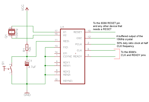
All microprocessors need a clock source in order to run and for the 8088 (and related processors), this is provided by the 8284 clock chip. This chip supplies the 8088 with a compatible clock signal (the 8088 needs its clock to have a 33% duty cycle) and also supplies it with 2 of it’s control lines – RESET and READY. The RESET signal does what it says on the tin and resets the 8088. This line can also be used by other peripherals on the computer so that they reset when the 8088 resets. The READY line is useful if you have some slow I/O interfacing to the processor. If your I/O needs to some extra time to deal with the processor’s request, it can take the READY line low. The processor will the wait for READY to go high again before resuming. Instead of connecting your peripheral to the 8088’s READY line directly, the 8284 provides 2 READY lines for your I/O (RDY1 and RDY2) which are synchronised the the system clock, and so you’d connect your I/O READY signal to one of them. Pins AEN1, AEN2 and ASYNC control the operation of RDY1 and RDY2. However, since the 8088’s peripheral chips are designed to work with it, they don’t need READY signals, so AEN1 and AEN2 are tied low and ASYNC is left floating.
The 8284 can take its clock source from either a crystal, or an oscillator, and you tell it which one via the F/C pin. If using an oscillator, the output of the oscillator is connected to EFI and F/C is tied high. If you’re using crystal (like me), then the crystal is connected across X1 and X2 and F/C is tied low. The oscillator is divided by 3 and given a 33% duty cycle and then output on CLK. Because the 8088 I have runs at 5MHz, I have used a 15MHz crystal.
The 8284 also provides a clock for peripheral devices on PCLK. This clock is at half the frequency of CLK and has a 50% duty cycle. The 8284 also provides a buffered output of the full oscillator frequency on the OSC pin.
The RES pin is an active low signal. Bringing this pin low tells the 8284 to output a reset signal. I’ve used a simple resistor and capacitor circuit to hold the system in reset for a short while after you switch on the power, to give time for the power supply and anything else in the circuit to stabilise. When the power is first switched on, the capacitor is discharged and so RES = 0V and the system is held in reset until the capacitor charges up and then the system is allowed to run. In my circuit, I’ve used a 10k resistor and 4.7uF capacitor, giving a power-on-reset time of 47us. The button then allows you to reset the system at any time.
The circuit diagram is shown below:
Testing the clock circuit
Testing the 8284 circuit is straightforward. With no chip and the power on, first check that the reset circuit works as expected. When the power is turned on, the output of the reset circuit should rise to 5V then stay there. Pressing the reset button should bring it down to 0V and when the button is released, the output should go back to 5V.
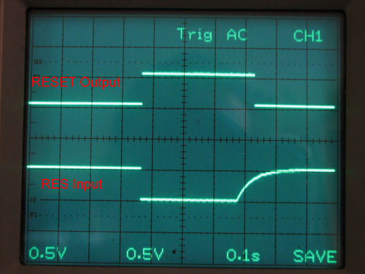
Once that’s done, plug in the chip and apply power then take a scope and check out the output pins. The RESET line should normally be low until the button is pressed. It should then remain high until the button is released, where it goes back low. The following photo shows my scope output of the RESET and RES lines (NOTE: I’m using 10x probes which is why the scope says 0.5V/div – 10*0.5=5 and so in actual fact it’s 5V/div)
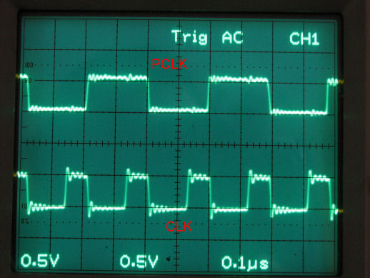
Next check the PCLK and CLK outputs. The CLK output should be a 5MHz square wave with 33% duty cycle, and the PCLK output should be a 2.5MHz square wave with a 50% duty cycle. The following photo shows my scope output of CLK and PCLK:
That wraps it up for the 8284 – the CLK, RESET and READY lines will be connected to the 8088 in the next step.
Adding the 8088 Processor
Now that the clock circuit is up and running, we need to prepare the 8088 for the next step, which is adding memory. This stage involves connecting the 8088 to the power supply and the 8284, and hard wiring some of it’s inputs.
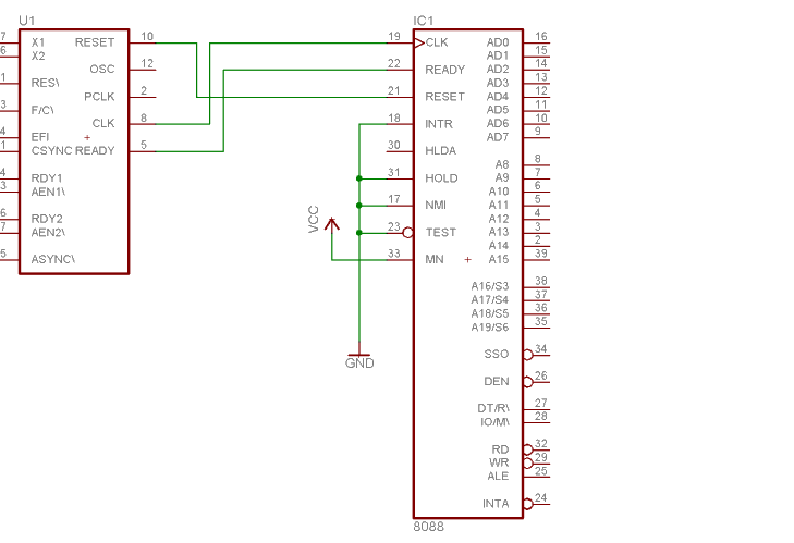
The 8284’s READY, RESET and CLK outputs should go to the 8088’s READY, RESET and CLK inputs. Next, the following pins should be tied to ground:
- NMI: Non-maskable interrupt. Taking this pin high will force the 8088 to call interrupt number 2 (interrupts will be handled later). The reason why this is called a non-maskable interrupt is because unlike all the other interrupts on the 8088, you can’t disable this one. For now, this pin is tied low until we play around with interrupts.
- INTR: Interrupt request. This pin is taken high if a device wants to trigger a particular interrupt on the 8088. For now, this is tied low.
- TEST: This pin is used as a debug tool. Basically, the 8088 has a command called WAIT. When the 8088 runs this command, it checks the status of TEST. If TEST is high, then the 8088 will wait and do nothing else (apart from respond to interrupts) until TEST goes low. In effect, TEST and WAIT can be used to add breakpoints in your code – you can pause execution at a particular point, then maybe have a snoop around the circuitry and see that everything is working as expected.
- HOLD: This pin is used if another part of the circuit needs to take control over the address and data buses and control lines. If HOLD is taken high, the 8088 tristates its address, data and control lines so that another device can use them. For this SBC, I don’t plan to use this, so it’s tied low.
- GND1, GND2: The 8088 has two ground lines, so be sure to wire them both.
The following 2 pins are tied high:
- MN/MX: Minimum/Maximum mode. The 8088 is designed to operate as a standalone processor or as one of a multiprocessing team. If MN/MX is tied high, the 8088 operates in minimum mode, where it’s got the whole computer to itself. If MN/MX is pulled low, the 8088 can chum up with other processors and share the workload. MN/MX changes how some of the control lines behave. This SBC is going to have just one processor and anyway, it’s simpler to work in minimum mode, so MN/MX is tied high.
- Vcc: Without power, the 8088 is just a cold, useless piece of silicon.
Below is a circuit diagram of the setup so far:
There’s nothing much to test here, apart from checking your wiring and making sure the correct voltage levels and signals are present on the pins connected.
Memory
As mentioned previously, one of the things which makes microprocessors so flexible is that you have complete control over how much memory you add and how it’s mapped. You can have as little or as much as you want (within limit of course) and arrange it how you see fit. Memory in the 8088 circuit will contain code, data, the stack and the 8088’s interrupt table. The memory is compromised of ROM and RAM. We need the RAM because we need space to store data and code which we can change while the processor is running. ROM is necessary because when the 8088 starts up, it has to have something to run, and so this is preprogrammed into ROM.
The 8088 has 20 address lines, which means it can address a whopping 1MB (!) of memory from 00000 to FFFFF. When the 8088 first powers up, it starts executing code from address FFFF0. This means there are 16 bytes of space to place our boot code. This is rather small, so what usually happens is that at FFFF0, we tell the 8088 to jump to somewhere lower down in memory where we’ve got a bit more breathing room.
Because we’ll be using two memory chips, we need some way to disable one chip and enable the other. We can’t have them both working at the same time – imagine what’d happen if the 8088 came to read from memory and both RAM and ROM dumped their outputs at the same time! Choosing which chip to enable is called address decoding. The memory configuration I’ve used is the same as the one described in Fuller’s book. This method is much simpler than the one used by Grossblatt because only a single NOT gate is needed to decode the address.
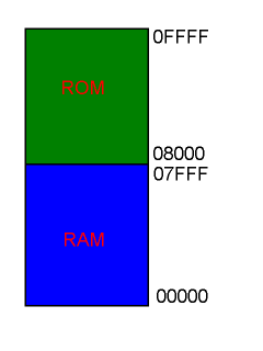
This configuration places 32K of RAM at the bottom of the address space (00000 – 07FFF) and 32K of ROM directly above it (08000 – 0FFFF).
Let’s have a look at the addresses in binary:
| 0000 0000 0000 0000 0000 | |
| 0000 0000 0000 0000 0001 | |
| 0000 0000 0000 0000 0010 | |
| . | RAM |
| . | |
| 0000 0111 1111 1111 1101 | |
| 0000 0111 1111 1111 1110 | |
| 0000 0111 1111 1111 1111 | |
| ——————————- | ——————————– |
| 0000 1000 0000 0000 0000 | |
| 0000 1000 0000 0000 0001 | |
| 0000 1000 0000 0000 0010 | |
| . | ROM |
| . | |
| 0000 1111 1111 1111 1101 | |
| 0000 1111 1111 1111 1110 | |
| 0000 1111 1111 1111 1111 | |
As we can see from this table, the only difference between a ROM address and a RAM address is address bit 15 – it’s 1 when it’s ROM and 0 when it’s RAM. This makes decoding very simple, because A15 can be connected directly to the RAM’s CS pin and connected to the ROM’s CS pin via one NOT gate.
The RAM and ROM chips themselves are relatively simple to work with. Both have a set of address and data lines which will connect to the address and data buses respectively. Both chips have a CS and RD pin. The CS pin is an active low signal. If CS is high, the chip is disabled and its outputs are tristated. When CS is low, the chip is enabled. RD is also an active low signal. If RD is taken low, the chip places the data present at the address specified. The RAM has an extra control pin which the 8088 will use: WR. As you can probably guess, this is an active low signal and used when you want to write a byte to RAM.
Decoding the address, data and control lines
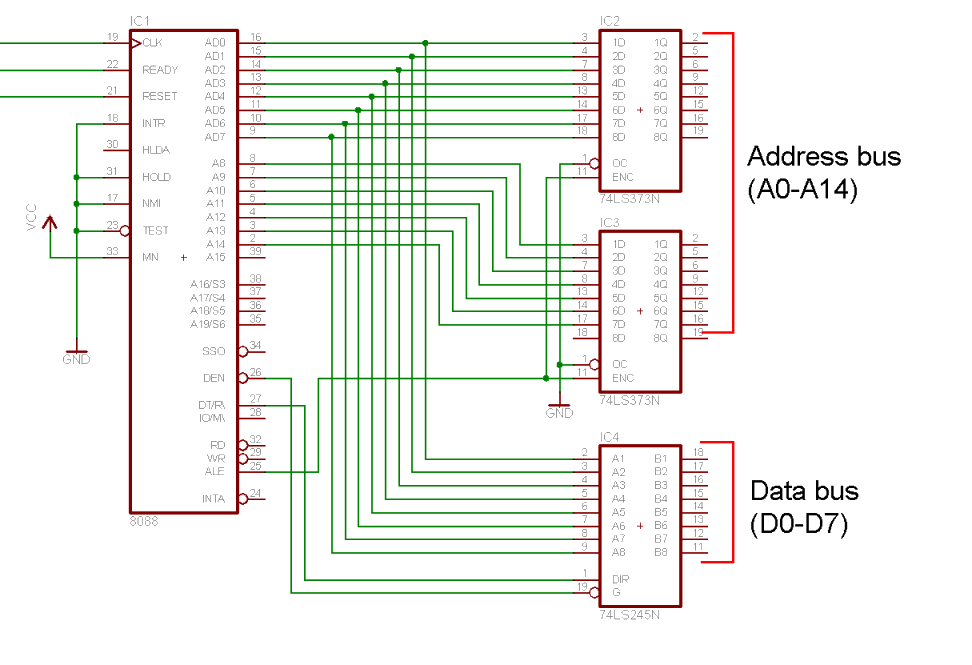
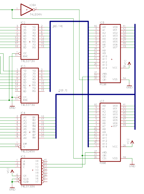
You’ll find that the 8088 doesn’t have separate address and data pins. In fact, the 8 data pins are multiplexed with the lower 8 address pins, and so there needs to be a way to separate the data from the address and indeed there is. When the 8088 places the address on the pins, it takes ALE high. We can use ALE to trigger a latch, which will then output the address and hold it there until a new address is present. A good candidate for this is the 74373 Octal latch. In this circuit the address bus is 15 bits wide, so we need 2 octal latches, and one of the inputs will be left unused.
Just as we can latch the address bus, the 8088 provides us with 2 output to tell us it wants to read or write data. These are DEN and DT/R. DEN is an active low signal indicating that the 8088 wants to manipulate data and DT/R tells us what it wants to do with the data. If DT/R is high, the 8088 is writing data and if it’s low, it’s reading data. A good chip to use for this case is the 74245 octal bus transceiver.
We can connect DEN to the chip’s E pin and the DT/R pin can go straight to the transceiver’s DIR pin. Now, when the 8088 want to read data, it places a low on DEN which enabled the 245 and also on DT/R, so data goes from B to A. If it’s writing data, DEN goes low again and DT/R goes high so data goes from A to B. It would therefore make sense for us to connect the A side to the 8088 and the B side to the rest of the circuit. The circuit diagram of the address latches and data transceiver is shown below.
The OC pins for the 373’s are tied low so that they’re outputs are always enabled.
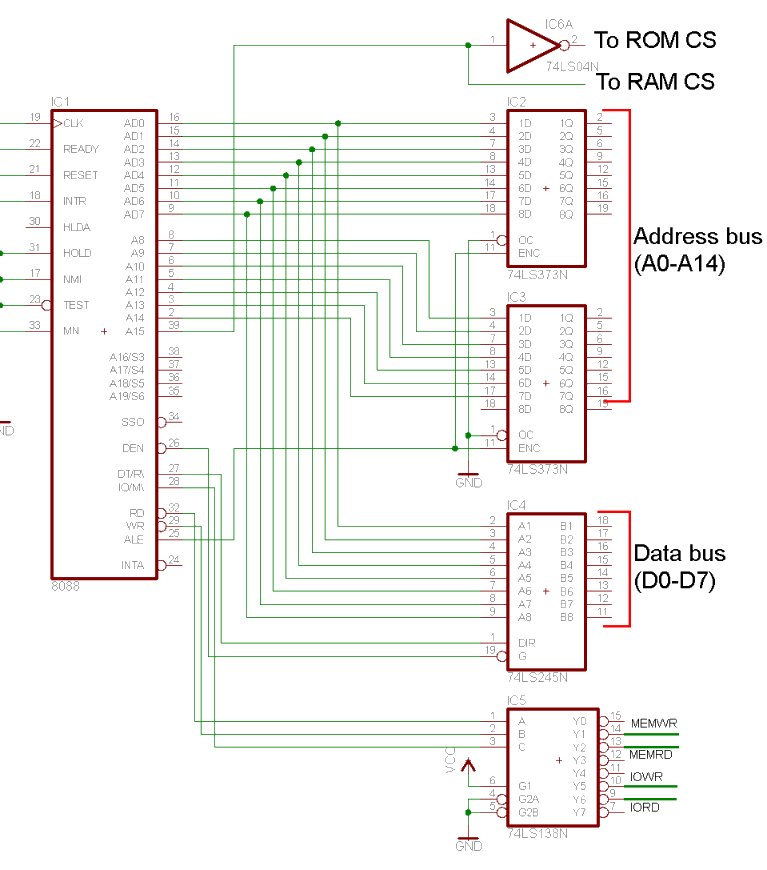
The last bit of decoding to do is the 8088’s control lines. There are three we need to deal with: IO/M, RD and WR. IO/M tells us if the 8088 is talking to I/O or memory. If it’s a high then it’s I/O and if it’s low it’s memory. RD and WR are active low outputs which tell us if the 8088 want so read or write data. Basically, we want to decode these to get IORD, IOWR, MEMRD and MEMWR. These should all be active low signals, because all the peripheral and memory chips need and active low signal to enable them.
| IO/M | RD | WR | |
| 0 | 0 | 1 | MEMRD |
| 0 | 1 | 0 | MEMWR |
| 1 | 0 | 1 | IORD |
| 1 | 1 | 0 | IOWR |
In this circuit, the 74138 1-of-8 decoder is used. With RD connected to A, WR to B and IO/M to C, we get the following outputs from the 138:
| MEMRD | O2 |
| MEMWR | O1 |
| IORD | O6 |
| IOWR | O5 |
MEMRD and MEMWR will be connected to the RAM and ROM RD and WR pins, respectively and likewise, IORD and IOWR will be connected to the RD and WR pins on I/O devices.
The following circuit diagram shows the 8088 with all its control lines decoded and everything ready and waiting for the memory:
Testing
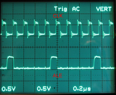
As with before, there isn’t really an amazing amount to test ere, apart from checking wiring and voltage levels. There is one test we can now do though. Now that we’ve got the 8088 all wired up, we power it up and scope the output of ALE. Pulses present on the ALE pin indicate that the 8088 has successfully powered up and is trying to read the code stored in address FFFF0. If you can see those on the scope, then that’s a good sign. The real testing comes when we’ve installed the memory and written some test code.
Now that all that looks like it’s working, it’s time to add ROM and RAM. For RAM, I have used a Winbond W24257A RAM chip, which is a 32Kx8. From ROM, I decided to use an Atmel AT28C256 32Kx8 EEPROM chip because I figured it’d be quicker to modify my programs, because unlike a UV Erasable EPROM, I don’t need to wait 15 minutes to erase the chip every time I want to modify my program.
For both chips, the address and data lines connect to the corresponding pins on the address and data latches. The MEMR signal goes to the chips’ OE pins and the MEMW goes to the RAM’s WE, because the ROM is read only. Finally, the ROM’s CS pin is connected to the output of the inverter in the above circuit diagram, while the RAM’s CS pin connects to the input of that inverter (i.e. Directly to A15). Below is the circuit diagram of the setup.
Writing software for the computer
The SBC is now at the stage where we can write software for it to test out it’s functionality. Because the processor is an Intel 8088, there are a lot of resources on the web that describe x86 assembly language. Robert Grossblatt’s book, The 8088 Project Book, which I recommended at the start has a chapter dedicated to 8088 assembly and is a good start. I also found 8086/8088/80286 Assembly Language by Leo J Scanlon (0132469197) on eBay and it has been a good reference.
In order to write software for the SBC, we’re going to need an x86 assembler that is capable of simply assembling the code and giving us a raw binary file. In Walter Fuller’s book, he suggests Borland’s Turbo assembler, TASM, and as I have a copy, I decided to use that. Now TASM is really old and in fact, I don’t think Borland support it any more, so I’ve uploaded my copy of TASM and TLINK so anyone interested in the project can write their own software.
The first piece of software I wrote for the 8088 was a RAM testing program. The program ran through each cell in RAM, wrote a unique value to it and then went back and read it again to check all was working.
Project Files
The schematic and code files for the project can be downloaded here:
This archive contains the following files (amongst others):
- 8088.sch: EAGLE schematic file
- asm.bat: Batch file to simplify the assembly/linking process. To use, simply run: asm.bat <file.asm>, where <file.asm> is the assembly file to build. A *.bin file is generated containing the assembled code.
- TASM.EXE, TLINK.EXE: BORLAND Turbo Assembler and Turbo Linker. These were used to compile the assembler files into machine code for programming into the 8088 EEPROM. NOTE: These are old Windows executables that will not run on modern Windows machines. You may need to use an emulator in order to get them working.
- template.asm: Template assembly file containing the basic code needed to get the computer up and running.
The archive also contains various test programs (in various stages of completion) that were used to experiment with various aspects
of the 8088 CPU.

marvellous page. I’m dreaming of building
an 8086 or 80186 computer that is different
from PC XT architecture. It’s my hobby to
collect info about everything connected with
retro comps.
I would like to thank you for the work being done here and the reference to great books which brought so much clear understanding to the 8088 and architecture. I built a similar circuit. My final desiring goal is to develope in the circuit an 8-bit ISA bus so that I can add the original IBM monitor adapter and write the INT 10H ISR. I have browsed the web and haven’t found hardware details as clear as the Grossblatt book.
Sounds very cool – when you finish your project, let me know! I agree, Robert Grossblatt’s book is great.
very nice page sir
i am actually doing this as hobby and bought the books they are really good
i am doing a more complex design more memory and fully buffered
i am not using DMA chip but i am using the logic design in the book also its in minimum mode it has two 8259
Great article, even if unfinished. I’ve recently purchased several Z80 (10MHz) and 80C186XL (25MHz) CPUs, with a view to first making a simple SBC, then something more complex with multiple processors, memory mapping and protection. I think with 10-15ns static RAM and some ‘373s for buffering reads over multiple clock cycles I could have 3 or 4 Z80 CPUs sharing the same memory, at full speed, without any contention (30 or 40MHz clock, 10MHz per CPU)… effectively creating a triple or quad port RAM. Would be more complicated with the 80186, but I’m looking forward to trying.
I’ve built a few Z80 SBCs from scratch, but this is the first time I’ll be doing it with an X86 proc. Thank you for the inspiration.
Glad you found the article useful, even in its unfinished state. Your project sounds very interesting: if you decide to publish it online, I’d love to hear about it.
In case anyone is interested, I’ve got some stuff I’d like give away (no free shipping though), before I put it on ebay.
– Amstrad PC200 parts (motherboard, keyboard, floppy drive; no casing, no transformer, no mouse).
– 1x 80C31 16Mhz processor (new, never used)
– 1x 80C32 12Mhz processor (new, never used)
– 4x Z80A cpus (new, never user; I’ve got smd versions to replace them)
– a few UV EPROMS (new, never used; 27C64, 27C256, 27C512; I’ve got smd eeproms to replace them)
– 2x 6264 8k 8bit SRams (I’ll keep the larger ones)
– 1x GBC (new. was intended to be used as an osciloscope but never did it)
Well email me if you are interested 🙂 I’ll send from Europe.
rui(.)martins(.)ds(at)gmail(.)com
Hi honestly its such a good article i have been searching web to find such a thing like this because i have a project that should be submitted in 2 days my project should be an 8088 computer system connected to 8255 ic the 8255 ic is connected to led matrix that should show up PSUT for now i have build up both the system and the led matrix as hardware and wrote an assemble code on an old dos computer and used a parallel port to send data to the 825 ic but what am looking for is how to burn this assembly code on my EEPROM and to make the system all over to work pleas i need help as fast as possible
Hello, I could help with a tutorial on how to create and load the ROM a simple prograpa, eg a LED turn on and off every few minutes
Hello , does anyone have a copy of the monitor program used in fullers book ? Please email it to me it would be greatly appreciated…
Tony – check this site
http://www.ee.nthu.edu.tw/jcliao/mic97/chap14R/showCh14R.htm
There are some programs for 8088 based computers
nice information but i want to ask how we can connet can bus with 8088 and how we program it?
Hi I LOVE this awesome tutorial but I was wondering if you could provide the schematics in a computer file, it looks like you are using cadsoft eagle so if you could provide the .sch files and any other necessary files like the library for the chips.
Thanks Justin
Thanks! Glad you like it. I’ve uploaded the schematic and code files that I have for the project. You’ll find it at the bottom of the article. Enjoy!
The power-on-reset time is 47ms instead of 47us, http://www.referencedesigner.com/rfcal/cal_05.php
Thanks for this, I was able to use this info to build intel 8088 based computer. It features 32k of SRAM and 32k of EEPROM (UV EPROM works as well). There’s an 8255 for parallel I/O, currently driving a hitachi style 4 line by 20 character LCD. An 8259A interrupt controller. A 82450 UART salvaged form old serial card for serial I/O. Currently the program reads the serial input and displays it on the LCD and echos it to the serial output – UART generates interrupt on byte received and computer reads it in. An 8253 timer is currently being used to generate 100 interrupts per second to count time since power on. All software is written in assembly, assembled with nasm, then written to EEPROM.
Photos: http://imgur.com/a/Bgh1l
Fantastic! Thanks for sharing!
How did you write to the eprom?
Very Cool!
Amazing tutorial.
Thank You the share..
hi,i tried to implement this schematic in proteus but i was unable to find any ic other than 8086.where can i download protues library for this project
CAN YOU PLEASE GUIDE ME HOW TO INTERFACE SINGLE ICS 256KB OF RAM AND 512KB OF ROM ON 8086. WITH PPI 8255A
NOTE ALL THE ABOVE RAM AND ROM ICS ARE SINGLE CHIP.
PLEASE EMAIL ME WITH SUGGESTIONS
AND ALSO I HAVE TRIED THIS IN PROTEUS BUT I AM NOT ABLE TO RUN YOUR PROGRAMMS
EMAIL ME mcitizen203@gmail.com if any one have any ides
Thanks for sharing so much great information.
I’m also starting to build an 8088 based on a finished project, but I bought the book you indicated to improve my knowledge.
When are you going to finish this project?
Good Stuff man! I wish you would continue this project. I fully understand though, life tends to get busy.